Chiplet-Based SoC Platform for Software-Defined Vehicles
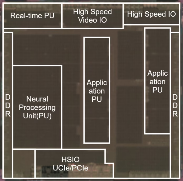
Renesas positions its new SoC technologies as the computing backbone for multi-domain ECUs that consolidate ADAS, infotainment, cockpit and gateway functions in software-defined vehicles. In SDVs, central high-performance compute platforms must run many applications in parallel while staying updateable over the air and meeting strict functional safety targets. To answer this, Renesas has developed three tightly linked innovations: a functional-safety-aware chiplet architecture, an AI-optimized 3 nm NPU design and highly granular power control across more than 90 power domains. These technologies feed into the R-Car Gen 5 family, including the R-Car X5H multi-domain SoC, which aims to give automakers a scalable platform from entry to premium vehicles with shared software assets. This approach supports modern E/E architectures that move away from many distributed ECUs toward centralized computing and zonal controllers, a trend also highlighted by broader SDV industry roadmaps.
Renesas builds on the industry-standard UCIe die-to-die interface but adds a proprietary RegionID mechanism to keep strict separation between multiple domains and workloads. By mapping RegionIDs into the physical address space and transporting them through UCIe, the SoC can enforce fine-grained access control via its MMU and real-time cores, achieving freedom from interference even when many software stacks run at once. Test results show a high inter-die bandwidth of 51.2 GB/s, which is close to the limit of intra-SoC communication and important for latency-sensitive ADAS and sensor-fusion tasks. Combining this bandwidth with robust partitioning allows multiple domains—such as autonomous driving, digital cockpit and connectivity—to share one multi-die platform without compromising ASIL-level isolation.
Functional Safety Architecture for ASIL D in Chiplet Designs
Meeting ASIL D in a chiplet-based automotive SoC is challenging because functional safety concepts must extend across dies, interfaces and shared resources. Renesas addresses this by designing its chiplet architecture from the ground up to support safety mechanisms across all dies, rather than treating chiplets as simple performance extensions. The RegionID-based scheme makes every access safety-aware, so applications from different domains cannot unexpectedly interfere with memory, peripherals or AI accelerators owned by another domain. This is critical as OEMs move toward domain and zone controllers that combine powertrain, body, ADAS and infotainment functions on shared compute nodes, an evolution echoed by other automotive semiconductor roadmaps.
Beyond logical isolation, Renesas emphasizes quality and defect screening, which are essential for automotive-grade reliability in large, advanced-node SoCs. Multi-layer clocking and test circuitry embedded into the hierarchical clock pulse generator structure let the company synchronize user and test clocks and adjust phases uniformly during validation. This enables zero-defect-oriented testing even as NPU sizes grow and clock trees become deeper, aligning with the automotive industry’s push for “near-zero” failures in safety-relevant compute platforms. Together with dual-core lockstep processing and independent power management for master and checker cores, the architecture helps detect faults promptly and supports compliance with ISO 26262 ASIL D requirements.
AI-Optimized 3 nm NPU Architecture for SDV Workloads
To keep pace with SDV use cases like sensor fusion, driver monitoring and immersive in-cabin experiences, Renesas has created a 3 nm SoC design that significantly scales NPU performance while preserving automotive-grade robustness. NPU areas have grown roughly 1.5 times compared with earlier generations, which increases clock latency and complicates timing closure across large arrays. Renesas counters this by breaking monolithic clock pulse generators into distributed mini-CPGs at sub-module level, shortening clock paths and simplifying timing for the AI fabric. This fine-grained clocking scheme helps the SoC sustain high AI throughput required for perception and prediction tasks while maintaining stable operation over the full automotive temperature and lifetime envelope.
However, adding more layers of mini-CPGs typically makes test clock synchronization harder, which can undermine fault coverage. Renesas integrates dedicated test circuits into the same hierarchical structure and routes user and test clocks through a unified signal path to simplify phase alignment. In test mode, upper and lower mini-CPGs synchronize under one clock source, enabling consistent timing and accurate defect detection across extensive NPU logic. This combination of AI performance and quality control supports the deployment of advanced driver-assistance and automated-driving stacks that demand both high compute density and strict functional safety assurances.
Granular Power Gating and Safe Power Monitoring
Renesas’ third pillar is an advanced power-control architecture that manages over 90 individual power domains to balance performance, efficiency and safety. The SoC can scale consumption from a few milliwatts up to tens of watts, depending on load, enabling always-on functions and heavy AI tasks to coexist while still meeting thermal and efficiency targets. To tackle IR drop issues that arise at smaller process geometries and higher current densities, the design splits power switches into ring PSWs and row PSWs, each handling a different phase of power-on behavior. The ring PSW suppresses inrush current during startup, while the row PSW equalizes impedance inside the domain, reducing IR drop by about 13 percent compared with conventional SoC designs.
For safety, the dual core lockstep configuration uses independent power switches and controllers for the master and checker cores, so a power-related fault on one side can be detected via divergent behavior. Loopback monitoring checks each power switch gate signal and confirms OFF states, helping identify stuck-on failures that could otherwise go unnoticed. A digital voltage monitor (DVMON) with strong resistance to temperature drift adds another layer of protection, improving aging tolerance by roughly 1.4 mV, which is important over the long life of vehicles. This blend of power gating, current management and monitoring contributes to both energy efficiency and dependable long-term operation in central SDV computers.
Role of R-Car X5H in Future Multi-Domain ECUs
These three technologies converge in the R-Car X5H SoC, which Renesas targets at multi-domain ECUs that centralize ADAS, autonomous driving, cockpit and connectivity workloads. The SoC’s chiplet-based scalability allows OEMs and Tier 1 suppliers to configure performance and AI capacity for different model segments without redesigning the fundamental platform.


