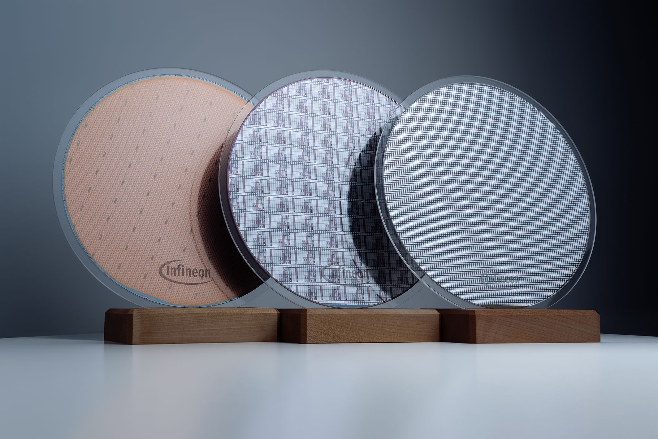

Infineon Technologies has processed functional power devices on 300-millimeter silicon carbide wafers. The company says this is the first such achievement in a full-scale semiconductor fab environment. The milestone was reached at its Villach facility in Austria and presented at electronica 2026 in Munich.
The development matters for e-mobility because silicon carbide helps convert electrical power with less loss. It supports traction inverters, on-board chargers, DC fast chargers, energy storage, and high-voltage vehicle systems.
Infineon’s Achievement
Infineon converted 300 mm SiC wafers into working power devices using existing silicon manufacturing equipment. This approach reduces the need to build an entirely new production environment for the larger wafer format.
A 300 mm wafer provides 2.3 times more chips than a 200 mm wafer. More chips per wafer can improve manufacturing efficiency and support a more secure long-term supply of SiC components.
The company describes the result as an early but important proof of industrial feasibility. It does not yet mean that 300 mm SiC production is fully ramped; Infineon will decide the technology roadmap and ramp timing with customers and partners.
Importance of Silicon Carbide
Silicon carbide is a wide-bandgap semiconductor material. Compared with conventional silicon, it can operate at higher voltages and temperatures while reducing power losses.
These characteristics allow power systems to become smaller, more efficient, and more power-dense. For electric vehicles, that can translate into more compact drivetrain components, reduced cooling needs, and improved use of available space.
Infineon positions SiC as a key technology for efficient power conversion. Its CoolSiC portfolio targets automotive, renewable energy, industrial, and AI data-center applications.
E-Mobility Applications
Traction Inverters
In an electric vehicle, the traction inverter converts DC power from the high-voltage battery into AC power for the electric motor. SiC devices can improve efficiency and power density in this central drivetrain function.
Infineon states that 1200 V CoolSiC MOSFETs in an electric drivetrain can reduce system size by up to 80 percent. Higher power density, lower cooling requirements, and fewer passive components contribute to this result.
Smaller drivetrain electronics can give vehicle designers more flexibility. They may also support greater cabin space, improved packaging, and more efficient use of the vehicle’s high-voltage architecture.
On-Board Chargers
An on-board charger recharges a plug-in hybrid or battery-electric vehicle while it is parked and connected to a charging point. It converts grid electricity into the voltage required by the vehicle’s high-voltage battery.
Infineon says its automotive CoolSiC 1200 V MOSFETs offer low electrical losses and strong robustness for automotive power conversion. These devices are intended for demanding high-voltage applications, including on-board charging.
The company also reports efficiency gains of up to 1 percent in the power-factor-correction and DC-DC stages of an on-board charger. Lower losses can reduce cooling requirements and support more compact charger designs.
DC Fast Charging
Public and fleet charging infrastructure also depends on efficient power conversion. Infineon says CoolSiC technology can cut charging time in half at the same charging-station footprint.
A single 1200 V SiC MOSFET can support an 800 V DC-link voltage. Infineon states that doubled power density can reduce the component count of a comparable silicon-based solution by 50 percent.
Lower conduction and switching losses can raise overall efficiency. This reduces the cooling effort needed in chargers, which is important for compact, high-power charging hardware.
A List of Key Benefits
- Larger 300 mm wafers yield 2.3 times more chips than 200 mm wafers.
- SiC reduces power losses during high-voltage power conversion.
- Higher power density enables smaller traction inverters and chargers.
- Reduced cooling needs can simplify thermal management in EV systems.
- Automotive CoolSiC devices support 800 V vehicle architectures.
- DC charging systems can deliver more power within the same footprint.
- SiC supports bidirectional charging and vehicle-to-grid use cases.
- The technology also serves solar, storage, industrial drives, and data centers.
Cold Split Adds Scale Potential
Infineon has also demonstrated Cold Split technology with 300 mm SiC wafers at its Dresden site. The process separates wafers from a SiC crystal boule with less material loss than conventional wire sawing.
Cold Split also reduces processing time. Infineon says the method can produce more wafers from the same crystal while requiring less capital expenditure.
For e-mobility, this could matter over time. More usable SiC material and more efficient wafer processing may help expand supply as demand grows for electric vehicles, charging networks, and grid-scale storage.
Supply Security and Industrialization
Infineon will continue executing its 200 mm SiC manufacturing roadmap. At the same time, it will plan the 300 mm SiC technology and its ramp schedule together with customers and partners.
This dual-track approach aims to balance near-term supply with future scalability. It also gives automotive customers a pathway toward advanced SiC technology without relying immediately on an unproven production transition.
The company frames the breakthrough as a foundation for secure, future-proof SiC supply. Its target markets include automotive, renewable energy, industrial applications, and AI data centers.
Infineon’s Wider Semiconductor Strategy
Infineon manufactures power semiconductors based on silicon, silicon carbide, and gallium nitride. The company announced a roughly €1.1 billion investment in a high-volume 300 mm GaN facility in Villach on 27 October 2026.
The SiC achievement extends the company’s 300 mm approach to a second wide-bandgap material. Infineon says this reinforces its position in semiconductor manufacturing innovation and supports profitable growth.
The announcement also follows Infineon’s broader focus on power systems and the Internet of Things. The company says its technologies support decarbonization and digitalization across mobility, energy, industry, and data infrastructure.
Sources: Infineon